SiC Diode Technology Benchmark Report (STMicro, Infineon, Onsemi)
Report Overview
First introduced commercially about 20 years ago, SiC Schottky Barrier Diodes (SBDs) have very low turn-on voltages (compared to Si PN diodes), negligible reverse recovery current due to unipolar carrier conduction, and are widely used in power electronics systems.
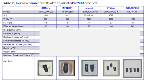
This report focuses on the five products shown in the Table below, evaluates the evolution of SBD structures, layouts, and electrical characteristics, and summarizes their technology trends.
The figure of merit (FOM: differential ON resistance per area, RF・A, VF, withstand voltage) are evaluated and correlated with device structural parameters, and compared with SiC MOSFETs.
Evaluated Product Specifications

Report contents and Summary of results
Detailed report contents are listed on page 2.
- Identification of device configuration (active area (SBD, JBS, MPS), peripheral edge).
- Extraction and comparison of N-Buffers structures against BPD (Basal Plane Dislocation) from major SiC manufacturers. – Thin N buffer layers from 0.2 μm up to 3 μm are observed, depending on the manufacturer’s experience and know-how (See page 3, Table 3-1).
- Analysis of the measured 1200V rated diode shows that the components of forward resistance RF are: (i) Epi layer resistance is 50-64%, (ii) N+ substrate resistance is 26%-33% of total RF. Therefore, the SiC substrate (N+) has a large impact on RF.
Note 1: Please contact us for current report pricing
Note 2: We are also planning to sell individual detailed reports for each of the above SBD products.
Please contact LTEC for details.


