Gate driver:Infineon 1EDI3020AS Priminaly IC Circuit Analysis Report
 |
 |
 |
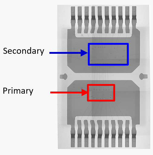
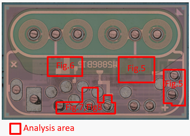
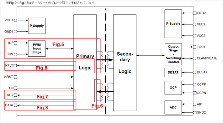
| Package X-Ray | Die image (Primary) | Function block |
Product features
- Single channel isolated IGBT driver using coreless transformer technology
- Compatible with IGBT up to 1200V
- Rail-to-rail output with peak current of 12A
- Propagation delay 60ns (Typ.)
Report summary
LTEC focus on the primary side chip of Infineon’s Gate Driver (1EDI3020AS), including (1) the signal processing circuit (Fig.5 Modulator) from the external input terminals INP and INN to the isolation element, (2) the circuit that processes the signal from the secondary side chip (Fig.6 Demodulator) and (3) output circuit of external output terminals NFLT, RDY, DATA (Fig.7,Fig.8 Signal Output Circuit). This is the partial circuit analysis report.
Report contents (91 pages)
- Installed chip size, chip photo (primary side chip)
- Partial circuit analysis of primary side chip (Modulator, Demodulator, and Signal Output Circuit)
- Deliveries: PDF report, schematic viewer, and EDIF data
Please contact us for report pricing.


