


CMOS Image Sensor:Samsung Galaxy S23 Ultra Main camera Structure, Layout analysis report
 |
 |
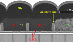 |
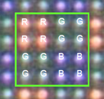
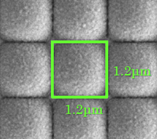
| Pixel OM image (S23 Ultra) | Pixel SEM image (S23 Ultra) | Pixel cross section image (S23 Ultra) |
Report summary
The stacked CMOS image sensor (CIS) for the main wide-angle camera of the Galaxy S23 Ultra is the world’s largest CIS at that time for smartphones with 200 million pixels, and is a product that uses Tetra2pixel and D-VTG technology.
Regarding this product, LTEC released a report that confirms the actual structure through physical analysis, and clarifies the applied technology, applied process, layout on the ISP side, etc. that are unknown in the datasheet.
LTEC also released main camera CIS analsysi report of he previous model Galaxy S22 Ultra, and comparison report of between S23 Ultra and S22 Ultra.
Product specifications/features
Product number : Galaxy S23 Ultra main camera CIS ISOCELL HP2 release date: April 2023
Galaxy S22 Ultra main camera CIS ISOCELL HM3 release date: April 2022
Report contents/Overview of results
- Galaxy S23 Ultra main camera CIS ISOCELL HP2 Structure, Layout analysis report (58 pages)
- Galaxy S22 Ultra main camera CIS ISOCELL HM3 Structure, Layout analysis report (50 pages)
- Structure, Layout comparison report of HP2 and HM3 (17 pages)
- Galaxy S22 Ultra main camera CIS uses vertical transfer gate (VTG), while Galaxy S23 Ultra uses dual vertical transfer gate (D-VTG).
- The Front-End process of the Galaxy S22 Ultra main camera CIS is manufactured at our own factory (Samsung-Fab.), but the Galaxy S23 Ultra is manufactured outside of our own factory.
See Foundry (Fab.) in report
Please contact us for report pricing.